Technology enables conversion of mobile phone cameras into high-resolution microscopes
-
 Loading...
 - Elizabeth Phua
- 04 May 2023
- 88 Views
- 0 Like
- 0 Comment
by Singapore-MIT Alliance for Research and Technology
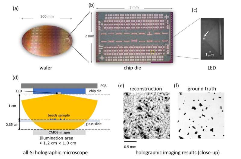
Researchers in Singapore have developed the world's smallest LED (light-emitting diode) that enables the conversion of existing mobile phone cameras into high-resolution microscopes. Smaller than the wavelength of light, the new LED was used to build the world's smallest holographic microscope, paving the way for existing cameras in everyday devices such as mobile phones to be converted into microscopes via only modifications to the silicon chip and software. This technology also represents a significant step forward in the miniaturization of diagnostics for indoor farmers and sustainable agriculture.
This breakthrough was supplemented by the researchers' development of a revolutionary neural networking algorithm that is able to reconstruct objects measured by the holographic microscope, thus enabling enhanced examination of microscopic objects such as cells and bacteria without the need for bulky conventional microscopes or additional optics. The research also paves the way for a major advancement in photonics—the building of a powerful on-chip emitter that is smaller than a micrometer, which has long been a challenge in the field.
The light in most photonic chips originates from off-chip sources, which leads to low overall energy efficiency and fundamentally limits the scalability of these chips. To address this issue, researchers have developed on-chip emitters using various materials such as rare-earth-doped glass, Ge-on-Si, and heterogeneously integrated III–V materials. While emitters based on these materials have shown promising device performance, integrating their fabrication processes into standard complementary metal-oxide-semiconductor (CMOS) platforms remains challenging. Read More…